UV-visible-NIR Microscope Design
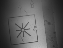
Contaminants on MEMS device only visible at 248 nm
UV Microscope Applications
NIR Microscope Applications
UVM-1 UV Microscope
UVM-1 NIR Microscope
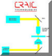
General diagram of a transmission UV-visible-NIR microscope

Silicon wafer with visible imaging

Silicon wafer with NIR imaging
The UV microscope and NIR microscope are designed to image in regions beyond the visible range. While the usable spectral range of each unit covers the UV, visible and near infrared regions, their optics and light sources may be optimized so that they are more effective in either the UV or NIR regions.
UV-visible-NIR Microscope Design
The standard model microscope, as commonly available, allows the user to image in the visible range only. For most modern microscopes that ranges from 420 to 700 nm.
A UV-visible-NIR range microscope covers a much larger spectral range and can image many things that are not visible to the eye. As with a standard microscope, the UV-visible-NIR microscope consists of light sources for transmission or incident (reflectance or fluorescence) illumination, optics to focus the UV, visible and NIR energy on the sample, more optics to collect and focus that energy on the imaging system and finally the imaging system that is sensitive in the UV or NIR regions.
The light sources are selected so that they have strong outputs in the ultraviolet and near infrared regions. The optics of such microscopes are made of materials that are transparent and can focus UV, visible and NIR range energy. And finally, the imaging systems are sensitive to either UV or NIR light in order to digitally store high resolution UV or NIR images.
Of course, such microscopes can be optimized for either the UV or NIR regions. Optimization entails changes in the light sources, optics and most importantly the imaging systems. The imaging systems selection is quite important as a silicon based system will not work in the near infrared region as the silicon is transparent there!
In fact, one of the most important uses for the NIR microscope is to image circuits and devices embedded within bonded silicon devices. Such devices consist of two silicon wafers that have been joined together and contain circuitry between them. As can be seen, imaging silicon with a standard microscope yields information only of the surface structure. However, in the NIR region, silicon is transparent and a NIR microscope can be used to image circuitry contained within the device.
UV microscope have many uses as well. They are commonly used for microscopy of contaminants that are transparent in the visible region but absorb light in the ultraviolet. This is especially important to precision industries such as those manufacturing OLED displays or semiconductor chips. Another vital application is imaging protein crystals. In drug discovery, protein crystals are grown to quickly develop new drugs. However, salt crystals also form in the same solution and cannot be differentiated by regular light microscopes. By using a UV microscope, the valuable protein crystals can easily be differentiated from the waste salt crystals.