How to Solve Thin-Film Thickness Measurement Challenges in Semiconductor Manufacturing
Every new generation of semiconductor technology introduces thinner films, smaller structures, and tighter process tolerances. Obtaining accurate thin-film measurements becomes far more demanding once critical wafer features shrink to only a few microns in size. Traditional inspection methods such as optical microscopy, profilometry, and standalone ellipsometry often provide either visual detail or analytical data, but rarely both with sufficient spatial precision. By merging high-resolution microscopy with spectroscopic analysis, microscope spectrophotometry enables semiconductor manufacturers to perform accurate thin-film thickness measurement directly on microscopic structures without physically altering the sample and on both transparent and opaque substrates.
Challenge 1: Navigating the Microscopic Map
Across every modern semiconductor wafer lies a dense network of microscopic structures, each needing careful inspection and precise characterization. Engineers may need to locate and measure a microscopic semiconductor feature several microns wide among layers of circuitry, dielectric films, and patterned materials on both opaque and transparent substrates. This generates a serious challenge for standalone thin-film thickness measurement systems, like standard benchtop reflectometry tools, that lack detailed optical imaging capabilities.
Microscope spectrophotometers integrate high-resolution microscopy directly into the measurement process, giving operators clear visual guidance during analysis. Users can view the sample and measurement aperture simultaneously, ensuring that the exact feature under investigation is also the feature being measured. The ability to confirm the sampling location visually improves the measurement reliability of complex semiconductor architectures.
Alongside this, microscope spectrophotometers enable precise isolation of extremely small sampling regions in complex semiconductor structures. Instead of averaging the data from adjacent semiconductor materials and patterned features, microscope spectrophotometers can focus on sub-micron spots to deliver more accurate thickness information from patterned wafers, narrow trenches, and highly localized structures. For semiconductor manufacturers, localized measurement targeting directly supports process control, defect analysis, and production consistency.
Challenge 2: Characterizing Multi-Layer Film Stacks
Inside advanced semiconductor devices, thin films are rarely deposited as single layers. Manufacturers rely on sophisticated stacks composed of oxides, nitrides, metals, and emerging proprietary materials. Measuring one individual layer within these stacks presents a significant analytical challenge because light interacts with every interface throughout the stack, leading to spectral responses influenced by multiple material boundaries simultaneously.
Through the collection of spectral data spanning ultraviolet, visible, and near-infrared wavelengths, microscope spectrophotometers help engineers evaluate complex multilayer film stacks at microscopic scales. To perform a thin-film thickness measurement, microscope spectrophotometers analyze how light reflects from or transmits through layered materials. The optical interactions between light and multilayer films generate interference patterns that contain valuable information about film thickness and material composition.
Using advanced optical modeling, the microscope spectrophotometer compares measured spectra with theoretical calculations to determine the thickness of individual layers. This process allows engineers to characterize complex stacks without physically sectioning the wafer.
New semiconductor materials often introduce optical behaviors that complicate thin-film thickness measurements and spectral analysis. Microscope spectrophotometers can address such issues through characterizing critical optical properties like refractive index and extinction coefficient across advanced thin-film stacks. These optical constants play an essential role in spectral modeling and thickness calculations, especially when manufacturers introduce new deposition chemistries and multilayer semiconductor materials. Non-destructive optical characterization ensures semiconductor manufacturers can strengthen process development, deposition validation, and long-term manufacturing consistency.
Challenge 3: Maintaining Yield Through Non-Destructive Analysis
Within semiconductor fabrication facilities, destructive testing methods such as cross-sectioning are valuable for failure analysis but inefficient for routine manufacturing metrology. Cutting or mechanically testing wafers consumes time, interrupts production, and destroys expensive materials, like semiconductor wafers or deposited thin films, that may still contain important process data.
Non-contact optical analysis is far more practical for semiconductor fabrication environments. Microscope spectrophotometers perform thin-film thickness measurements without touching the wafer surface, lowering the risk of contamination or physical damage during inspection.
Automation further expands the capabilities of microscope spectrophotometry in semiconductor manufacturing environments. Advanced systems can perform automated mapping routines within multiple wafer locations, generating localized thin-film thickness data capable of revealing deposition non-uniformity and early signs of process drift. Measurements collected from multiple wafer locations reveal process variation early enough to prevent yield-impacting inconsistencies.
Microscope spectrophotometers can offer more than localized thickness measurements alone. The combined imagining and spectral analysis workflow can reveal contamination, scratches, coating non-uniformity, and localized wafer defects throughout routine analysis. This integrated approach supports faster semiconductor analysis while improving process consistency.
Integrating Microscope Spectrophotometers Into the Workflow
Semiconductor fabrication facilities operate under constant pressure to expand analytical capability without sacrificing space or disrupting established production workflows. Microscope spectrophotometers expand the functionality of existing optical microscopy systems and reduce the need for additional standalone metrology equipment in semiconductor cleanrooms.
Existing microscopy infrastructure can enable thin-film thickness measurement, spectral analysis, and microscopic imaging in a single workflow, simplifying wafer characterization and decreasing equipment redundancy across the laboratory. Digital imaging collected alongside spectroscopic data also improves traceability by linking measurement results directly to a specific sampling location on the wafer surface. The result is a more organized analytical process that delivers repeatability, strengthens validation efforts, and improves production documentation within semiconductor manufacturing environments.
Advanced Semiconductor Analysis With Microscope Spectrophotometers
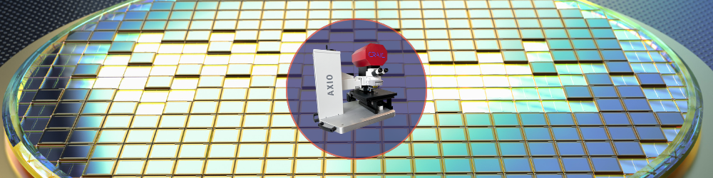
Semiconductor laboratories in need of localized thin-film thickness measurement and optical characterization can depend on the microscope spectrophotometry solutions developed by CRAIC Technologies. Our 2030XL PRO™ Microscope Spectrophotometer integrates microscopic imaging with spectral analysis to support advanced wafer characterization, multilayer film analysis, and semiconductor process evaluation at microscopic scales. Reach out to our experts to find out more about our 2030XL PRO™ Microscope Spectrophotometer and how it can refine semiconductor process analysis at microscopic scales.
References
- Calleja M, Encinar M, Kosaka P, et al. Spatially Multiplexed Micro-Spectrophotometry in Bright Field Mode for Thin Film Characterization. Sensors. 2016;16(6):926. doi:10.3390/s16060926.
- CRAIC Technologies. Microspectroscopy for Thin Films, Defect Analysis, and Heterostructure Imaging. AZoMaterials. https://www.azom.com/article.aspx?ArticleID=23898. Published 26th August 2024. Accessed 20th May 2026.