Streamlining Wafer Inspection: The Role of Microscope Spectrophotometers in Thin Film Thickness Metrology
Wafer inspection has entered a phase of precision as semiconductor manufacturers continue scaling device architectures beyond the limits of traditional planar design. Thin films must now be measured across microscopic regions packed with multilayer structures, narrow trenches, and dense circuitry. Microscope spectrophotometers streamline this process by combining targeted optical microscopy with spectroscopy for extremely localized thin film thickness analysis on sophisticated semiconductor wafers.
The Technical Gap in Thin Film Metrology
Traditional metrology tools struggle to satisfy the spatial precision needed for modern semiconductor manufacturing. Conventional spectrophotometers typically measure areas several millimeters wide, making them useful for blanket films but far less effective for patterned production wafers. A large measurement spot collects reflected light from multiple structures simultaneously, including dielectric layers, metal lines, active circuitry, and scribe marks. The resulting data offers an average across unrelated regions rather than the thickness of a single microscopic feature.
Spectroscopic ellipsometry delivers excellent sensitivity and direct film thickness measurements, yet its angled illumination geometry produces size limitations during inspection of densely packed structures. Because light reaches the wafer surface at an oblique angle, the measurement spot becomes elongated instead of tightly circular and with a much larger sampling area. Narrow trenches and isolated transistor structures become difficult to analyze since the beam cannot fully access confined geometries without introducing shadowing effects.
Microscope spectrophotometers overcome such geometric constraints through normal-incidence optical microspectroscopy. The instrument directs light perpendicular to the wafer surface, producing a circular micron-scale measurement spot that can be positioned precisely on specific wafer coordinates.
Key advantages of microscope spectrophotometers include:
- Precise targeting of microscopic device features
- Reduced interference from surrounding wafer regions
- Improved compatibility with three-dimensional architectures
- Better process monitoring on patterned wafers.
How Microscope Spectrophotometers Determine Film Thickness
Precision optics combined with interference-based spectral analysis enable microscope spectrophotometers to determine thin film thickness. When measurements are performed, broadband light passes through a microscope objective and is focused onto the wafer surface from a perpendicular angle. The perpendicular illumination geometry improves targeting precision while minimizing distortions associated with angled metrology systems.
As light reaches a thin film, part of the beam reflects from the top surface, and another portion travels through the film and reflects from the underlying substrate interface. These reflected waves return with different phase relationships depending on wavelength and optical path length. Certain wavelengths interfere constructively, producing stronger reflected intensity; others interfere destructively and reduce reflected intensity. This interaction generates oscillating spectral patterns known as interference fringes.
The integrated spectrophotometer captures these patterns across ultraviolet, visible, and near-infrared wavelengths. Advanced software algorithms then compare the measured spectra against theoretical optical models containing refractive index and extinction coefficient data for the material stack under analysis. Through iterative fitting calculations, the software is able to identify the thickness value that most accurately matches the measured spectral response.
Because the measurement process relies entirely on optical analysis, engineers can perform repeated inspections during fabrication without damaging production wafers or interrupting manufacturing flow.
Applications of Microscope Spectrophotometers in Wafer Inspection
Microscope spectrophotometers are widely used for localized thin film thickness measurements on patterned semiconductor wafers. Manufacturers can position micron-scale measurement spots directly onto transistor regions, dielectric features, interconnects, and other confined device structures that are difficult to isolate with conventional large-area metrology systems, allowing localized thin film measurements on specific semiconductor features like gate oxides, metal interconnect layers, and memory stacks.
An additional area microscope spectrophotometers are applied to is the inspection of three-dimensional semiconductor architectures. High-aspect-ratio trenches, stacked memory layers, and deep divas demand optical measurements within narrow and vertically complex geometries. Normal-incidence optical microspectroscopy allows light to reach such structures more directly, improving measurement reliability across advanced wafer topographies.
Wafer-scale thickness mapping represents another important application in semiconductor process monitoring. Automated X-Y stages and high-speed spectral acquisition systems enable rapid collection of localized thickness data across 300 mm wafers. Engineers use these measurements to evaluate film uniformity, monitor deposition consistency, and identify process variations associated with Atomic Layer Deposition (ALD) and Chemical Vapor Deposition (CVD) fabrication workflows.
Alongside this, microscope spectrophotometers are used for deep ultraviolet thin film analysis. Shorter wavelengths provide greater optical sensitivity for ultra-thin dielectric layers and photoresist coatings below 10 nm, supporting detailed characterization of advanced semiconductor materials and deposition processes.
Broader Analytical Versatility in the Fab
In addition to localized thin film thickness measurements, microscope spectrophotometers support several other optical characterization applications within semiconductor fabrication environments. The integration of microscopy with full spectral analysis allows manufacturers to evaluate microscopic contamination, reflectance variation, and surface roughness across highly confined wafer regions.
These spectral analysis capabilities also extend to complex multilayer semiconductor structures. Through refractive index and optical constant modeling, manufacturers can analyze material composition, layer interactions, and optical behavior simultaneously, enabling the deeper evaluation of thin film performance within advanced semiconductor devices like Gate-All Around (GAA) transistors, Vertical NAND (VNAND) memory structures, photonic devices, and multilayer interconnect architectures.
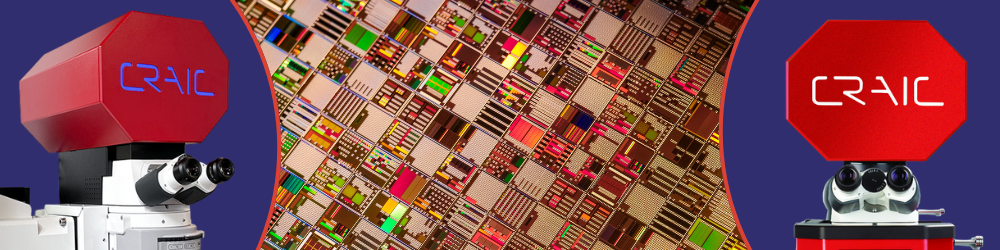
Precision Wafer Metrology Solutions from CRAIC Technologies
CRAIC Technologies develops microscope spectrophotometer systems specifically for microscopic optical analysis within semiconductor fabrication workflows. The 2030PV PRO™ and 2030XL PRO™ platforms integrate proprietary Lightblades™ spectrometers capable of rapid, low-noise spectral acquisition from the deep ultraviolet through the near-infrared. Combined with Lambdafire™ control software and specialized FilmPro™ analytical modules, these systems support multilayer thickness measurements, automated spectral mapping, and 5D surface characterization on sub-micron sample areas. We also incorporate NIST-traceable standards to improve measurement consistency across advanced wafer inspection workflows. Speak to our specialists now for additional insights on our products and how they fit into thin film metrology and advanced wafer inspection workflows.
References
- Swanepoel R. Determining refractive index and thickness of thin films from wavelength measurements only. Journal of Optical Society of America A. 1985;2(8):1339-1343. doi:10.1364/JOSAA.2.001339.
- Calleja M, Encinar M, Kosaka P, et al. Spatially Multiplexed Micro-Spectrophotometry in Bright Field Mode for Thin Film Characterization. Sensors. 2016;16(6):926. doi:10.3390/s16060926.