Raman Spectroscopy of Semiconductors
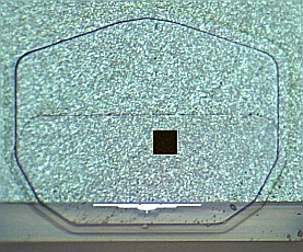
Raman microspectrometers are used to identify contaminants on precision devices.
![]()

Raman spectrum of a silicon device
Raman microspectroscopy is used to identify contaminants, measure silicon crystal structure and stress in silicon structures.
Contamination analysis is a difficult problem for any failure analysis laboratory. It is especially challenging if the contamination has occured in a supposedly clean environment. Raman spectroscopy, especially Raman microspectroscopy, is essential in identifying the contaminants once they have been located. Raman spectroscopy is ideal due to its small sampling and the fact that it is a vibrational technique with the ability to identify many organic components.
Silicon Crystal Form: Raman spectroscopy can measure the difference between different crystal stuctures of Silicon. For example, there are variations in the Raman spectra when comparing polycrystalline to amorphous silicon.
Strain in Silicon Structures: Raman spectroscopy detects strain in silicon structures by measuring the lattice vibrations sensitive to strain. This makes it the perfect tool for such applications as monitoring wafers.
To learn more about Raman microspectroscopy, select one of the following links:
The Science of Raman Microspectroscopy
Raman Microspectrometer Design